


A Shift in Semiconductor Manufacturing
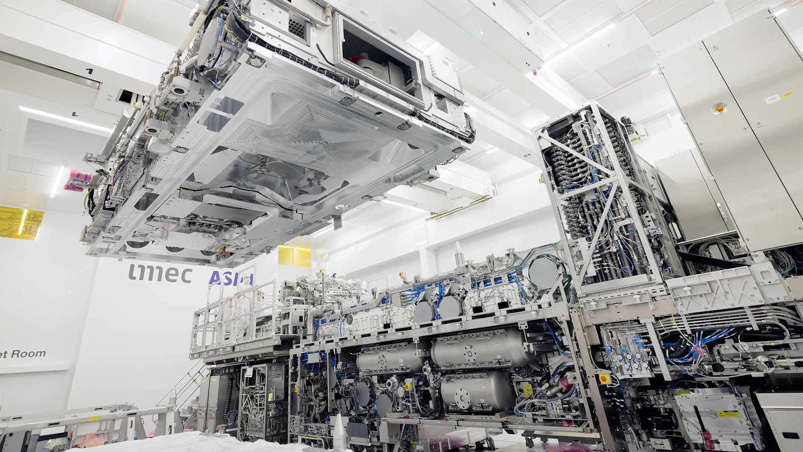
ASML Holding NV has secured critical commitments from global semiconductor leaders Samsung Electronics Co. and Taiwan Semiconductor Manufacturing Co. (TSMC) to adopt its latest High NA EUV (Extreme Ultraviolet) lithography equipment. This move marks a significant milestone in the industry’s attempt to keep pace with the explosive global demand for artificial intelligence infrastructure, according to Bloomberg.
The High NA EUV machines, which cost approximately $400 million each, are essential for manufacturing the most advanced AI accelerators. Samsung plans to integrate this technology into its memory chip production by 2028, while TSMC intends to begin adoption for high-volume manufacturing by 2030.
The Transition to 12-Inch Photomasks
Beyond adopting the new machinery, the industry is preparing for a fundamental shift in the technology format for photomasks. Photomasks act as the templates for printing circuit patterns onto silicon wafers using light. The industry currently relies on a 6-inch standard, but the group has agreed to transition to 12-inch versions.
This change is designed to increase throughput by 40% and simplify the design process, according to Marco Pieters, ASML’s chief technology officer. By moving to larger masks, chipmakers aim to overcome physical limitations that have previously forced them to rely on complex, costly vertical stacking and multi-patterning strategies.
Strategic Implications for Industry Leaders
The commitment from TSMC—which accounts for roughly 16% of ASML’s revenue—is particularly significant. TSMC has historically been cautious about the high cost of these machines, questioning whether productivity gains justified the investment. However, the company has now agreed to build a test line for 12-inch masks by 2031, with full production implementation targeted for 2033.
For Samsung, the move is a dual play. As both a leading memory chip manufacturer and a contract logic chip producer, the firm is positioning itself to address the ongoing global shortage of memory chips driven by AI data center requirements. Samsung stated it would collaborate with industry partners to develop the necessary infrastructure to support this transition.