


A Pivot to Purpose-Built Silicon
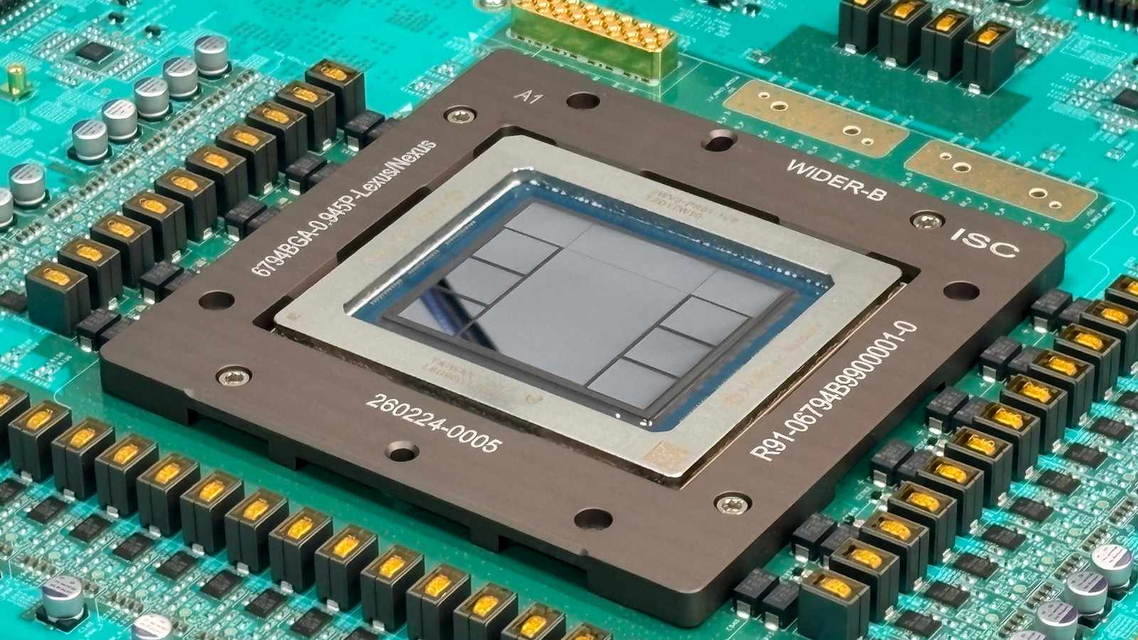
OpenAI officially unveiled its first custom-designed inference ASIC, codenamed Jalapeño, at the Hot Chips 2026 conference. Developed in collaboration with Broadcom, the chip represents a strategic departure from relying exclusively on general-purpose GPU clusters, signaling the company’s intent to optimize its infrastructure specifically for the high-demand, low-latency requirements of modern agentic AI workloads.
During the technical presentation, OpenAI’s engineering leads—Richard Ho, Ravi Narayanaswami, and Chris Leary—detailed a rapid nine-month development cycle. From initial register-transfer level (RTL) design in late 2024 to a late 2025 tapeout, the project utilized internal AI-driven hardware design tools to accelerate the physical implementation process. The resulting silicon is a 3nm-class ASIC manufactured by TSMC, specifically architected to handle the distinct phases of an LLM request: compute-bound prefill, latency-sensitive draft generation, and memory-bandwidth-bound verification.
Performance and Efficiency Benchmarks
OpenAI framed Jalapeño’s performance against industry-standard NVIDIA hardware, specifically the GB200 and GB300 systems. Utilizing the ‘InferenceX’ benchmark, the company reported that Jalapeño achieves significantly higher ‘mixed tokens per second per kilowatt.’ For instance, on the DeepSeek R1 670B model, the chip demonstrated roughly 1.7x higher throughput per kilowatt and 3.6x lower end-to-end latency compared to the GB300, while operating at a 700-watt TDP against the competitor’s 1,400-watt rating.
The architecture relies on 216 GiB of HBM4 memory per package, reportedly supplied by Samsung, providing 15.4 TB/s of bandwidth. By keeping key-value (KV) cache states local within the chip and gating unused compute units during specific inference phases, OpenAI claims to have solved the power-efficiency bottlenecks common in heterogeneous GPU fleets where underutilized accelerators continue to draw significant baseline power.
Strategic Implications
The introduction of Jalapeño highlights a broader trend among frontier AI labs to vertically integrate their hardware stacks. By controlling the silicon and the software stack—specifically the ‘Gluon’ programming framework—OpenAI aims to bypass the limitations of standard CUDA-based development. This allows the firm to map, place, and schedule workloads using its own models, rather than relying on manual kernel optimization.
However, the project faces clear constraints. The chip is strictly an inference engine and is not designed for the intensive training workloads where NVIDIA’s platforms remain dominant. Furthermore, as a TSMC N3-based product, Jalapeño competes for the same advanced wafer and packaging capacity as NVIDIA’s upcoming Blackwell and Rubin lines. With second-generation designs already reaching tape-out and a third generation in development, OpenAI is signaling an aggressive, multi-year commitment to proprietary silicon to sustain its model-serving economics.